Constrained shrinking of pre-stressed films to achieve high-resolution nanoscale patterns
Tech ID
21-060
Inventors
P. R. Selvaganapathy
S. Abosree
Patent Status
PCT application filed
Stage of Research
Proof of principle
Contact
Glen Crossley
Associate Director, Business Development and Intellectual Property
Abstract
Nanoscale pattern formation which enables precise reproduction of features below 100 nm is critical for many applications, including semiconductors, nanoelectromechanical systems, and as textured surfaces for biomedical applications. Current methods of nanofabrication include nanoimprint lithography (NIL), which can produce nano patterns of high density and high resolution.1 However, NIL requires the fabrication of a master mold using focused ion beam lithography or electron beam lithography, which are time-consuming and expensive processes.2 Another route to nanofabrication is thermal nanoimprinting (also known as hot embossing), where pre-stressed films are thermally nanoimprinted and shrunken. However, upon shrinking the imprinted topographical features are lost due to material recovery.3 Therefore, there is a need for more efficient methods to produce nanoscale patterns.
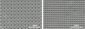
Researchers at McMaster have combined thermal nanoimprinting with a new shrinking approach, constrained shrinking, which retains shrunken patterns and enables fabrication of high resolution, uniform, and large area patterns at dimensions below 50 nm. This process can be tuned to obtain rectangular features from a square or ellipsoid patterns from circles. Additionally, repeating the constrained shrinking process has the potential to extend the resolution.4,5 The shrunk patterns can be repurposed as their own molds, allowing for continuous cycles of shrinkage to sub 10 nm.
Applications
- High resolution uniform patterns for industrial applications (ex. semiconductor manufacturing, microsystems, optoelectronics)
- To develop optical structures such as gratings, laser components and other micro/nanoscale structures
- Potential replacement for deep UV and phase shift masking technologies for semiconductor chip manufacturers of chips with 40 – 160 nm technology
Advantages
- Low-cost and simple fabrication of high-resolution uniform patterns
- Preservation of pattern height
- Tuneable miniaturization to achieve different patterns and dimensions from a single master mold
References
- Sayed, et al. Nanotechnology. 2021, 32, 505301. https://doi.org/10.1088/1361-6528/ac244d
- Pimpin, et al. Eng. J. 2012, 16, 37–56. https://doi.org/10.4186/ej.2012.16.1.37
- Zhu, et al. Sensors Actuators A. 2013, 195, 21–6. https://doi.org/10.1016/j.sna.2013.02.015
- Sayed, et al. Nanoscale Advances. 2020, 2, 5461 – 5467
- Sayed, et al. Microsystems and Nanoengineering. 2021 (accepted)
Image obtained from Reference 1.